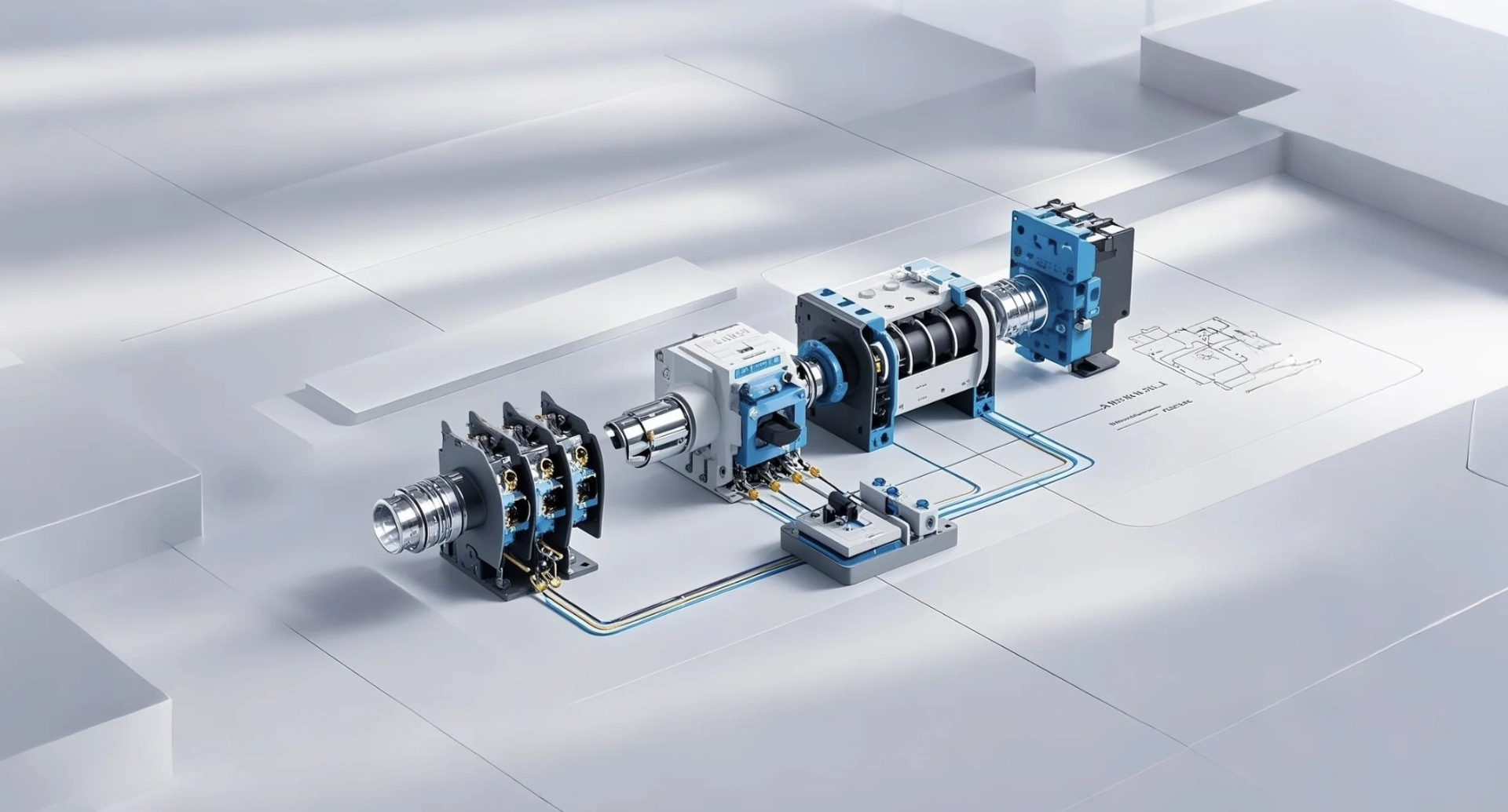
Semiconductor materials are useful because engineers can precisely control the number and motion of electrical charge carriers inside them. Crystal composition, doping, electric fields, light, temperature, and device geometry can change conductivity in predictable ways. That controllability makes rectification, switching, amplification, sensing, light emission, and energy conversion possible in compact, manufacturable devices.
Calling a semiconductor merely “something between a conductor and an insulator” is a useful first approximation, but it misses the engineering advantage. The important feature is not a fixed middle level of resistance. It is the ability to create energy bands, junctions, interfaces, and channels whose carrier behavior can be designed and modulated.
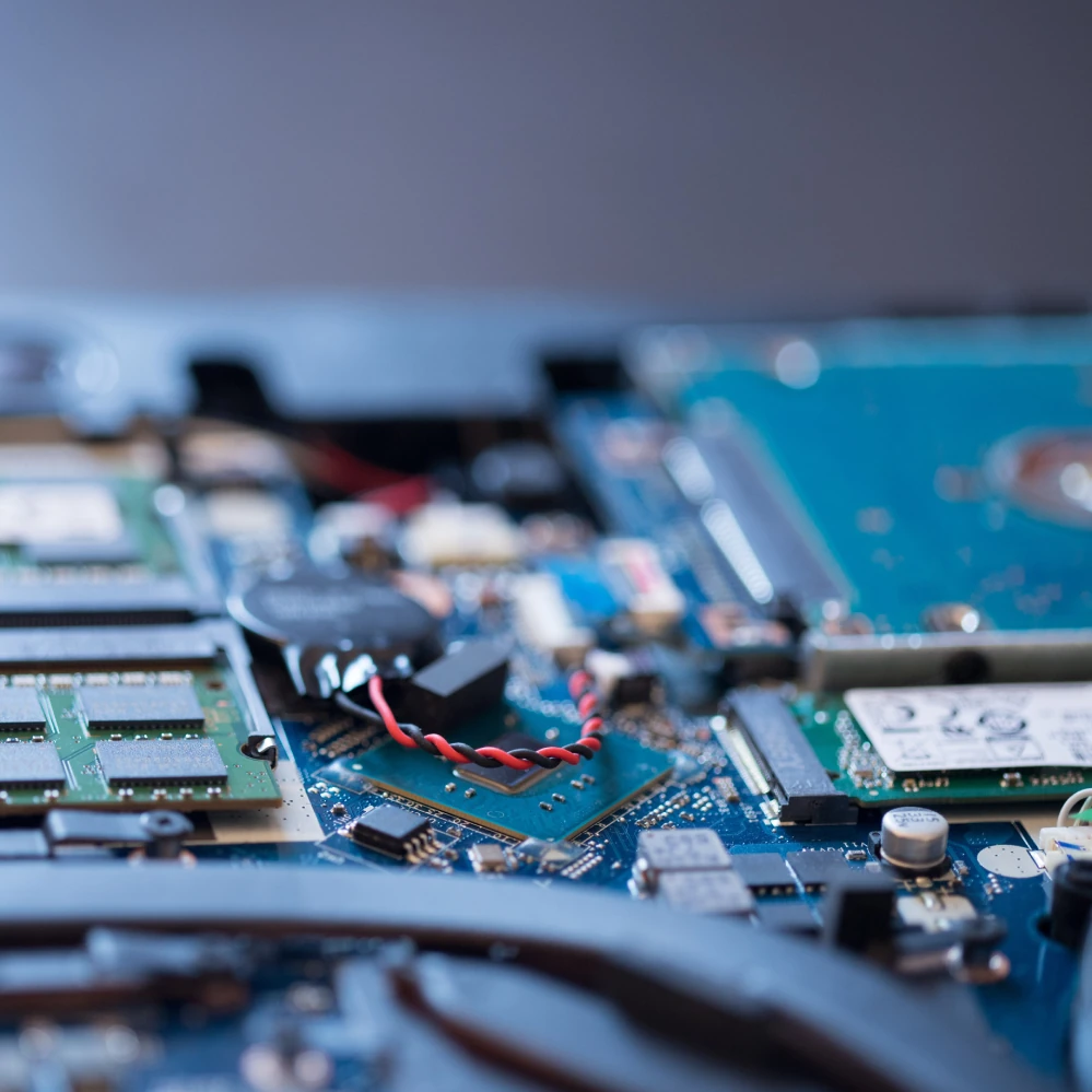
Energy bands make controllable conduction possible
In a solid, closely spaced atoms produce ranges of allowed electron energy called bands. The valence band contains states associated with bonding, while the conduction band contains states in which carriers can move through the material. The energy separation between them is the bandgap.
In an insulator, the bandgap and available carrier population make normal conduction extremely small. In a metal, available states allow charge to move readily. In a semiconductor, the band structure permits a useful carrier population that can be changed by doping, temperature, illumination, electric field, and carrier injection.
Electrons promoted into the conduction band can carry current. The corresponding absence of an electron in the valence band behaves as a positively charged carrier called a hole. Device physics tracks both carrier types, their concentration, mobility, generation, recombination, and movement under electric fields or concentration gradients.
Doping creates n-type and p-type regions
A pure semiconductor has an intrinsic carrier concentration set largely by material and temperature. Manufacturers add controlled impurity atoms to change carrier concentration and the position of the Fermi level. Donor dopants create n-type material in which electrons are the majority carriers; acceptor dopants create p-type material in which holes are the majority carriers.
Doping is not the same as mixing in a bulk conductor. Concentrations, depth profiles, activation, crystal defects, diffusion, and interfaces must be tightly controlled. Modern fabrication uses processes such as ion implantation or diffusion followed by thermal treatments, with metrology and statistical process control to keep electrical parameters within limits.
Junctions and fields turn material into devices
Diodes
When p-type and n-type regions meet, carriers diffuse and leave a depletion region with a built-in electric field. Applying forward bias lowers the junction barrier and increases current strongly. Reverse bias widens the depletion region and usually produces only small leakage until a breakdown mechanism becomes significant.
A real diode is not a perfect one-way switch. It has forward voltage, dynamic resistance, leakage, junction capacitance, recovery behavior, temperature dependence, power loss, and specified breakdown limits. Designers choose rectifier, Schottky, Zener, photodiode, LED, or other structures according to the circuit function.
Transistors
A transistor uses a control input to influence a larger current or voltage. In a MOSFET, the electric field from an insulated gate changes the carrier population in a channel between source and drain. In a bipolar junction transistor, carrier injection and transport across junctions allow base drive to control collector current.
Transistors can operate as digital switches, analog amplifiers, power converters, oscillators, current sources, and many other building blocks. Their behavior is continuous and physical rather than perfectly binary: threshold spread, on-resistance, leakage, capacitance, gain, switching loss, temperature, and safe operating area all matter.
Optoelectronic and sensing devices
Photodiodes and image sensors convert absorbed photons into electrical signals. Solar cells separate photogenerated carriers to deliver power. LEDs and laser diodes use electron-hole recombination to emit light; direct-bandgap compound semiconductors are particularly valuable for efficient emission. Temperature, magnetic field, pressure, chemicals, and radiation can also change electrical behavior in structures designed as sensors.
Why silicon became the mainstream platform
Silicon combines useful electrical properties with abundant raw material, mature wafer production, scalable fabrication, and a stable native oxide that supports high-quality insulated-gate structures. Decades of process development, equipment, design tools, packaging, reliability data, and supply infrastructure reinforce its economic advantage.
That does not mean silicon is best for every device. Its strengths are part of a manufacturing system. A material with a more attractive isolated property may still lose at product level because substrates are costly, defects reduce yield, contacts are difficult, thermal interfaces are weak, or the packaging cannot exploit the theoretical advantage.
Why engineers choose other semiconductor materials
- Germanium and silicon-germanium: useful where carrier transport and heterojunction performance support high-speed or specialized devices, with process and leakage tradeoffs.
- Gallium arsenide and indium phosphide: important in radio-frequency, microwave, photonic, and optical-communication applications because of their electronic and optical properties.
- Silicon carbide and gallium nitride: wide-bandgap materials used in power and high-frequency applications where higher electric-field capability, switching performance, or high-temperature potential can justify different substrates, drivers, layouts, and packaging.
- Organic and amorphous semiconductors: useful for selected displays, sensors, photovoltaic, and flexible or large-area devices, with mobility, stability, uniformity, and lifetime tradeoffs.
Wide-bandgap devices do not improve a power converter automatically. Gate drive, parasitic inductance, switching speed, insulation, electromagnetic emissions, thermal path, protection, connector choice, and PCB layout determine whether the system realizes the device’s potential. Faster edges can reduce switching loss while increasing ringing and EMI if the interconnect is poorly controlled.
A practical material-selection framework
Start with the required function and operating envelope, then compare candidates across the complete product:
- Electrical target: voltage, current, frequency, gain, noise, leakage, switching loss, and efficiency.
- Material properties: bandgap, carrier mobility, critical electric field, thermal conductivity, and optical response.
- Device structure: junction, channel, contact resistance, oxide or interface quality, die area, and edge termination.
- Thermal design: transient and steady-state junction temperature, heat spreading, interface material, cooling, and temperature cycles.
- Manufacturing: wafer size and quality, process maturity, yield, test coverage, packaging, assembly capability, and traceability.
- Reliability: mission profile, derating, wear-out mechanisms, humidity, contamination, radiation where relevant, and qualification evidence.
- Commercial factors: availability, second sources, lifecycle, intellectual property, cost, and supplier change control.
System integration should include the board and connector path. High-current power devices require low-resistance conductors and robust thermal interfaces; high-speed devices require controlled return paths and low parasitic discontinuity. Teams can review PCB connector integration options early rather than treating interconnects as a late mechanical detail. For geometry, pinout, shielding, or packaging constraints that catalog parts cannot meet, create a requirement set before evaluating custom connector solutions.
From datasheet claim to qualified component
A datasheet rating is meaningful only under its stated conditions. Review test circuits, junction or case temperature, pulse duration, mounting, cooling assumptions, and derating. Confirm whether maximum ratings are survivability boundaries rather than recommended operating points. Compare typical curves with guaranteed limits and account for lot and temperature variation.
Qualification should reflect the application mission profile. Device-level electrical and environmental tests, package-board interaction, thermal cycling, vibration where applicable, powered endurance, and system fault tests answer different questions. Record exact part revision, date or lot code, board, firmware, test equipment, uncertainty, and acceptance criteria so results can support a production decision.
Common misconceptions
- “Semiconductor” means a fixed halfway resistance: conductivity can span a wide range and is deliberately controlled.
- A diode is a perfect one-way conductor: real devices have loss, leakage, capacitance, and breakdown limits.
- A transistor is only on or off: analog behavior and switching transitions are central to practical design.
- The material with the best headline property wins: interfaces, process yield, package, reliability, and cost can dominate.
- A higher voltage rating solves the system: switching dynamics, thermal impedance, drive, layout, and protection remain critical.
FAQ
Why can temperature change semiconductor behavior?
Temperature changes carrier generation, mobility, leakage, threshold-related behavior, and material and package resistance. The direction and magnitude depend on the device, so designers use temperature-dependent curves and qualified limits rather than one room-temperature value.
What is the difference between n-type and p-type material?
Doping makes electrons the majority carriers in n-type material and holes the majority carriers in p-type material. Combining and arranging these regions creates junctions and device structures with controllable electrical behavior.
Why are GaN and SiC called wide-bandgap semiconductors?
Their bandgaps are wider than silicon’s. Along with other material properties, this supports devices suited to high electric fields, power conversion, high frequency, or elevated temperature. Actual system benefit still depends on device design, packaging, layout, drive, cooling, and reliability.
Are all electronic components made from semiconductors?
No. Electronic assemblies also use metallic conductors, ceramic and polymer insulators, magnetic materials, resistive films, electrolytes, optical materials, and mechanical structures. Semiconductor devices perform many active control and conversion functions, but they operate inside a broader material system.
Takeaway
Semiconductors power modern electronics because their carrier behavior can be engineered. Doping, junctions, electric fields, geometry, and material choice transform that controllability into practical devices. The right selection comes from balancing physics with fabrication, packaging, reliability, supply, and the real operating mission.